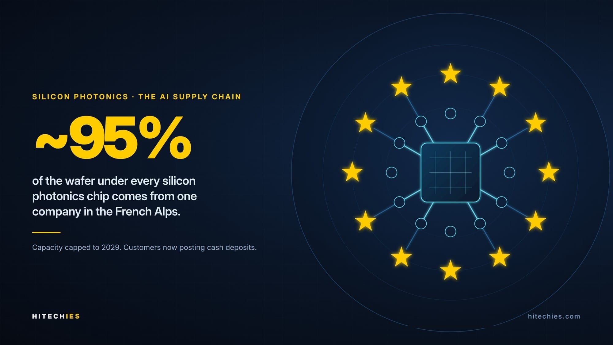
The most important chokepoint in the AI buildout right now isn't in Santa Clara or Hsinchu. It's in a valley outside Grenoble. Soitec, a French chip-materials company most people outside the industry have never heard of, makes the engineered wafer that sits under almost every silicon photonics chip shipping today. By UBS's estimate, it holds around 95% of that market. And it has just started locking its customers into multi-year contracts with cash deposits attached — the clearest signal yet that the AI bottleneck has moved past the GPU.
What actually happened
Soitec is negotiating capacity reservation agreements with more than ten photonics customers, and CEO Laurent Rémont says roughly 80% of them should be signed within weeks. The terms are unusually hard for a materials supplier:
- Fixed pricing over the contract period
- Cash deposits tied to committed volumes — refunded if the customer takes what it promised, forfeited if it doesn't
- Renegotiation triggers if a customer wants more than its committed volume
- Mandatory inventory data sharing, so Soitec can see whether customers are over-ordering
That last clause is the interesting one. A supplier only demands visibility into customer inventory when it has been burned by a phantom demand cycle before — which Soitec has, badly, in RF-SOI for smartphones. It's the behaviour of a company that believes the demand is real but refuses to build capacity on the strength of a purchase order alone.
The numbers behind it: Photonics-SOI revenue passed $100 million in the fiscal year ended March 2026, ahead of plan. Guidance is for that to more than double in FY27 — above $200 million — and Rémont now describes that figure as "absolutely a floor." In the June quarter, Photonics-SOI sales doubled year-on-year while the Edge & Cloud AI division grew 46% to €65 million, on group revenue of €113 million. The stock has nearly quadrupled this year.
Why copper ran out of road
The physics is not subtle. Inside an AI cluster, passive copper is still the cheapest, lowest-latency way to move data — but only to about five metres, and that ceiling tightens as per-lane rates climb through 100G and 200G. Beyond it, you need active electrical cables with DSPs burning power, or you go optical. Marvell's own framing is that essentially every connection from five metres to two kilometres inside a modern data centre is already carried by PAM4 DSP-based optical modules.
Now scale that. A cluster with hundreds of thousands of accelerators needs an all-to-all fabric where any GPU can talk to any other at close to memory bandwidth. The link count and the number of switch tiers both climb as the cluster grows, while the rack budget for power and thermal headroom does not. Optics stops being a cost line and becomes the thing that decides whether the cluster can be built at all.
That's the argument behind co-packaged optics — moving the optical engine off the faceplate and onto the switch package itself. Nvidia's Quantum-X and Spectrum-X Photonics switches claim 3.5x better power efficiency, 4x fewer lasers, 63x better signal integrity and 10x network resiliency versus pluggable optics. Quantum-X (InfiniBand) was slated for late 2025; Spectrum-X (Ethernet) for 2026. Whatever discount you apply to vendor numbers, the direction is settled: the industry is committing capital to light.
Where the substrate sits
A silicon photonics chip is a waveguide problem before it's a transistor problem. Light has to be confined in silicon and kept from leaking into the bulk wafer underneath, which means a buried oxide layer held to extremely tight thickness uniformity across a full 300mm wafer. That's what Photonics-SOI is, and it's why the market hasn't fragmented so far: the wafer isn't a commodity input, it's a process the rest of the flow is calibrated against. Requalifying a substrate means requalifying the PDK, the foundry process and the customer's product — a multi-year exercise nobody undertakes casually. The barrier is switching cost and qualification time rather than anything unrepeatable, which matters for how long you should expect it to hold.
So the chain looks like this, and Soitec sits at the very front of it:
-
Photonic substrate Soitec (Photonics-SOI)Dominant ~95%
-
Lithography & tools ASML, Zeiss, AixtronDominant
-
Process R&D / PDKs imec (BE), Luceda (BE), Ligentec (CH)Strong
-
PIC foundry TSMC (COUPE), UMC, Tower, GlobalFoundries (Fotonix), CanSemi — plus X-FAB, Smart Photonics in the EUSub-scale
-
Lasers & optical components Coherent, Lumentum, Innolight, Eoptolink, BrowaveWeak
-
CPO packaging & assembly Foxconn, Fabrinet, SPIL, TFC — PHIX (NL), X-Celeprint (IE) at low volumeWeak
-
Switch / system Nvidia, Broadcom, Arista, CiscoAbsent
Bars show the strength of the European position at each layer, from Dominant (five) to Absent (one). Value capture rises as you move down the list; European ownership falls.
The European read
This is the shape of European semiconductor strength in miniature, and it's worth being honest about what it does and doesn't buy.
Europe owns the entrances. Substrates, lithography, deposition tools, design kits, foundational research at imec — these are genuine chokepoints, hard to replicate, protected by decades of accumulated process knowledge rather than by policy. Nothing in an AI data centre gets built without passing through them.
Europe does not own the exits. The value capture happens where the optical engine is packaged onto the switch and sold as a system, and that is Taiwan, Singapore, Japan and the United States. TSMC's COUPE platform is in production; UMC shipped its first mass-produced silicon photonics wafers from Singapore in July 2026 and plans its own platform in 2027; Tower is converting its Arai fab in Japan to 300mm silicon photonics for Q4 2027; GlobalFoundries bought Singapore's Advanced Micro Foundry outright in 2025. The European PIC ecosystem — X-FAB, Smart Photonics, PHIX, Ligentec — is real and improving, but it is running pilot-line and specialty volumes while the hyperscale flow goes elsewhere. Smart Photonics raised €100 million from ASML, NXP and other investors to scale indium phosphide production; TSMC spends more than that in a fortnight.
The EU is trying to close the gap. Chips Act 2.0 explicitly names photonics and integrated photonics as critical technologies, and Photonics21 has proposed eight Grand Challenge Projects at €250–900 million of public money each, which it argues would leverage into a €6–8 billion programme. The earlier photonixFAB initiative, €48 million led by X-FAB, is the template. These are serious numbers by European standards and rounding errors by hyperscaler standards.
And there's a wrinkle in the sovereignty story worth noting: the newly qualified Photonics-SOI high-volume line isn't in France. It's in Singapore. Soitec says no new plant before 2029, that an unequipped building in Singapore could add capacity within 6–12 months, and that no US facility is planned "at this stage." A European chokepoint that expands in Asia to serve American customers is a more accurate picture of how this industry actually works than any Chips Act press release.
The reframe for investors
"AI infrastructure" has stopped being a synonym for one company. The stack that actually has to work, in order:
GPU→HBM→Advanced packaging→Scale-up networking→Optics→Substrate→Power & cooling
Each layer has a different capacity ceiling, a different lead time and a different concentration risk. Worth walking it with the numbers attached, because the numbers are what tell you where the constraint is sitting this quarter.
1. The unit of compute is now the rack
An Nvidia GB300 NVL72 puts 72 GPUs into a single fully-connected scale-up domain and draws up to 142 kW in one liquid-cooled rack — eight power shelves at 33 kW each. That is roughly twenty times what a conventional enterprise rack was provisioned for. Once you accept that framing, most of the interesting engineering stops being about the die and starts being about everything that feeds it and everything that connects it.
2. HBM: bandwidth per FLOP, not FLOPs
HBM4 runs a baseline of 8 Gb/s per pin, with Nvidia targeting around 22 TB/s from a 12-high stack and per-stack capacity landing anywhere from 12 GB to 64 GB depending on stack height and die size. Micron has said its entire 2026 HBM4 output is sold out; Samsung began shipping to Nvidia early in 2026; SK hynix still holds the majority of the market. The thing to understand is that HBM isn't a separate bottleneck from packaging — every additional stack consumes interposer area and TSV throughput, so memory and packaging constrain each other.
3. Advanced packaging: the interposer is the real estate
CoWoS is the layer where HBM stacks and logic dies get married onto one substrate, and it has been the hard ceiling on accelerator output for two years running. TSMC does not guide to CoWoS capacity, so the working numbers here are supply-chain estimates rather than disclosure: trade press and analyst trackers put end-2026 capacity in the region of 130,000–140,000 wafers a month, with the supply–demand gap reportedly narrowing from around 20% to 10% across the year. Treat the figure as directional. Narrowing, not closed — and every generation that adds HBM stacks or moves to larger reticle-stitched interposers eats the new capacity as it arrives.
4. Scale-up vs scale-out: the 18x cliff
This is the part that explains everything downstream. Inside the NVL72 rack, fifth-gen NVLink gives each GPU up to 1.8 TB/s, with nine switch trays aggregating 130 TB/s of fabric. Step outside the rack and each GPU gets a ConnectX-8 NIC at 800 Gb/s — 100 GB/s once you convert bits to bytes. That's roughly an 18:1 drop the moment a tensor has to cross a rack boundary. Both figures come straight from Nvidia's published NVL72 reference architecture; the ratio is ours, and it compares peak per-GPU link bandwidth in each direction rather than achieved application throughput, which will be lower on both sides.
Which is exactly why the scale-up domain stops at 72 GPUs: it stops where copper stops. The whole 142 kW, liquid-cooled, cable-backplane design exists to keep those 72 GPUs inside passive copper reach. Push the domain to 144 or 576 GPUs and the copper budget breaks, so the interconnect has to become optical — and an optical scale-up fabric is a fundamentally different (and much more expensive) machine.
5. Optics: the fabric grows faster than the lane rate
Now do the arithmetic on a serious cluster. A hundred thousand GPUs at 800 Gb/s each is 80 Pb/s of edge bandwidth before you count the switch tiers above them.
It's worth resisting the tempting shorthand that collective traffic "scales quadratically." It depends entirely on topology, collective algorithm and parallelism strategy — ring and tree all-reduce are designed precisely so that per-GPU bandwidth cost stays roughly flat as the domain grows, which is why data-parallel training scales at all. Three more specific things do grow, and they're what actually drive the optics bill:
- Tiers. Holding full bisection bandwidth as node count rises means adding switch layers. Each tier inserts another optical hop into every cross-domain flow, so transceivers per GPU climbs even when bytes per GPU doesn't.
- Flow count. The all-to-all exchanges that mixture-of-experts routing depends on generate on the order of N² distinct flows across N endpoints. Per-node bytes may hold roughly constant, but the messages get smaller and more numerous, which turns the problem into congestion control and tail latency rather than raw throughput.
- Reach. Every GPU added past the copper boundary is an optical link that didn't exist before, at a fixed cost in modules, lasers and faceplate power.
Against that, SerDes lane rates roughly double every two years with power per bit improving about 30% per generation — real progress, but on a slower and more predictable curve than cluster size has been growing. Optics is where the gap between those curves gets paid for.
Co-packaged optics is the response: shorten the electrical path from a faceplate module to a few millimetres of package trace and you recover most of the SerDes power. Nvidia's claimed 3.5x power efficiency and 4x fewer lasers are that trade, expressed as marketing. The engineering consequence is that the optical engine becomes part of the switch package — which drags substrate quality, laser attach and packaging yield into the critical path of a networking product.
6. Substrate: one qualified supplier, and a capacity ceiling
Under all of that sits Photonics-SOI — around 95% of it from one company, on UBS's estimate rather than any company disclosure. Soitec has said it does not expect to build a new plant before 2029, with near-term expansion limited to installing tools in existing cleanroom space and reallocating output between product lines. Worth reading that as what it is: a stated commercial plan, revisable if the economics change, not a law of nature.
Still, it makes this layer behave differently from the ones above it. HBM, packaging and foundry capacity can all be relieved by spending money on a roughly two-to-three year horizon, and the money is already committed. Here the incumbent has chosen not to, which is why the capacity reservation contracts with forfeitable deposits exist at all — if you can't build the supply, you ration it and make the customer post collateral. (Power, at the far end of the chain, is slower still and for entirely different reasons.)
It's worth being precise about what kind of position that is, because "monopoly" is doing a lot of work in most write-ups. Soitec is the dominant qualified supplier, not the holder of a physical impossibility. Nothing in the physics says only one company can polish a buried oxide to that uniformity; what protects the position is that the qualification cycle runs into years and nobody redesigns a shipping transceiver to chase a second source while they're allocation-constrained. That's a real moat, and it is a moat with a clock on it — the lead is measured in qualification cycles, not in decades.
Which means the timeframe you're underwriting matters more than the market share number:
- 2026–28: genuinely extraordinary leverage. Customers are locked in, capacity is capped, alternatives aren't qualified, and pricing power is being converted into contracts with deposits attached.
- 2029–30+: a 95% share at premium pricing is the single loudest funding signal you can send to bulk-silicon and alternative-substrate programmes. By the time Soitec's own new capacity arrives, so does theirs.
7. Power and cooling: the layer capex can't fix
And then the constraint leaves the semiconductor industry entirely. Large power transformers were running at 128–144 weeks in Wood Mackenzie's Q2 2025 buyer survey — 128 for standard units, 144 for generator step-up — with NEMA quoting up to three years and trade reporting putting specialised 765 kV class units past four. Five years ago these shipped in four to six weeks. Lead times vary widely by voltage class, buyer and whether you hold a slot, so read these as a range rather than a price list. Medium-voltage switchgear is 26–32 weeks standard and 50–80 weeks for custom AI-campus configurations. Prime-power gensets are around 18 months with the major OEM order books full into 2028. Grid interconnection queues average about five years, with more than 2,000 GW of generation and storage sitting in them.
No amount of money compresses a 144-week transformer or a five-year interconnection study. That is a different class of constraint from a fab tool order, and it is why the marginal AI data centre is increasingly sited by where the power is rather than where the customers are.
The pattern
The binding constraint moves because each layer scales on a different curve. Compute scales with transistor density and interposer area. Interconnect scales with SerDes rate — a slower, more predictable curve than the growth in tiers, flows and reach it has to absorb. Power scales with civil engineering and regulatory process, which don't respond to capex at all. It was HBM. It was CoWoS. Right now, in the interconnect layer, part of it is a wafer made by one company in the Alps; at the far end, it's a transformer with a three-year lead time.
The single number that keeps pushing the constraint down-stack is bytes moved per FLOP. Larger models, longer contexts, mixture-of-experts routing and more aggressive tensor and expert parallelism all raise it. As long as that ratio keeps climbing, value keeps migrating away from the compute die and toward whatever is currently hardest to move bytes through. Buying the accelerator vendor is a proxy for the whole stack only for as long as the accelerator is the scarce thing.
What would break this
Three things to watch, because the bull case here is not risk-free.
Double-ordering. Soitec's insistence on inventory transparency is a tell. If hyperscalers and transceiver makers are booking capacity at multiple points in the chain against the same end demand, the correction is violent. LightCounting sees a credible path to $100 billion in annual AI-cluster optics sales by 2030 — Ethernet transceiver sales doubled in 2024, grew 70% in 2025 and are tracking around 60% in 2026 — but explicitly frames a "bumpy ride" scenario alongside it, and this industry has a long history of cycles rather than straight lines.
Substrate substitution. A 95% share is a target, and this is the risk that decides the 2029-onward case rather than the next eight quarters. Bulk-silicon and alternative-substrate approaches will get funded precisely because the incumbent now has pricing power and a capped supply. Soitec's own history is the cautionary example: its bonded SmartSiC process for silicon carbide was undercut by cheap bulk substrates out of China, and analysts covering the stock have written the expected SmartSiC ramp out of their forward estimates entirely, leaving capacity built for it badly under-loaded. Process advantages in this business are durable until suddenly they aren't.
The rest of the company. Photonics is still well under a fifth of Soitec's revenue. The rest — RF-SOI for smartphones, imager wafers, automotive — has been shrinking, with group revenue down 34% in FY26 and mobile down 41%. The photonics story is real; whether it arrives fast enough to carry the group depends on how much of the legacy decline is a cycle and how much is structural.
Nothing here is investment advice — it's a supply-chain read. Figures are from company reporting and cited third-party estimates as of August 2026.
Where the headline numbers come from
Not all of the figures above carry the same weight. Company disclosure, third-party estimate and vendor marketing claim are three different things, and it should be obvious which is which:
Photonics-SOI >$100m in FY26, guided to more than double in FY27
Company disclosure
Soitec FY26 results and Q1 FY27 revenue release. Reported figures.
Capacity reservation terms; deposits; 10+ customers; ~80% signing
Company statement to press
CEO Laurent Rémont, Reuters, Aug 2026. Not yet in a filing; contracts described as close to signature, not signed.
~95% Photonics-SOI market share
Third-party estimate
UBS. Soitec publishes no share figure. A single-analyst estimate of a small, opaque market.
No new plant before 2029
Statement of intent
Rémont, Reuters. A revisable commercial plan, not a physical ceiling.
1.8 TB/s NVLink; 800 Gb/s ConnectX-8; 142 kW rack
Vendor specification
Nvidia NVL72 reference architecture. Peak link rates, not achieved throughput.
The 18:1 bandwidth cliff
Our calculation
Derived from the two Nvidia figures above after unit conversion. Peak-to-peak ratio.
~22 TB/s per 12-Hi HBM4 stack; 2026 capacity sold out
Vendor target + company statement
Nvidia target figure and Micron's own sold-out comment, via trade press.
Transformer 128–144 weeks; ~5-year interconnection queues
Survey & regulatory data
Wood Mackenzie Q2 2025 survey; NEMA commentary; LBNL Queued Up 2025. Wide variance by region and voltage class.
$100bn AI-cluster optics by 2030
Third-party forecast
LightCounting, explicitly framed as one scenario against a "bumpy ride" alternative.
130,000–140,000 CoWoS wafers/month by end-2026
Supply-chain estimate
Trade press and analyst trackers. TSMC does not guide to CoWoS capacity. The weakest-sourced number here.
3.5x power efficiency, 4x fewer lasers, 63x signal integrity
⚠ Vendor marketing claim
Nvidia, on Spectrum-X / Quantum-X Photonics. Comparison baseline unspecified. Discount accordingly.
Dots show how directly the figure is evidenced — four for reported company numbers, one for a marketing claim. Cards are ordered strongest evidence first; the ⚠ marked figure is the one to lean on least.
Sources
- Soitec — FY2026 full-year results
- Soitec — Q1 FY2027 revenue
- Reuters — Soitec locks customers into multi-year deals as AI wafer demand surges
- Nvidia — Spectrum-X Photonics co-packaged optics switches
- Marvell — copper and optical interconnects in AI clusters
- TrendForce — silicon photonics foundry landscape
- EE Times — a silicon photonics supply chain for Europe
- optics.org — Photonics21 on Chips Act 2.0
- LightCounting — $100 billion market for AI cluster optics by 2030?
- Nvidia — NVL72 AI Factory reference architecture, system components
- Blocks & Files — HBM4 supply takes shape
- TrendForce — TSMC CoWoS supply-demand gap
- AI data centre supply chain lead times (Wood Mackenzie, NEMA, LBNL data)